Co-reporter:Nicholas D. Eastham, Alexander S. Dudnik, Thomas J. Aldrich, Eric F. Manley, Thomas J. Fauvell, Patrick E. Hartnett, Michael R. Wasielewski, Lin X. Chen, Ferdinand S. Melkonyan, Antonio Facchetti, Robert P. H. Chang, and Tobin J. Marks
Chemistry of Materials May 23, 2017 Volume 29(Issue 10) pp:4432-4432
Publication Date(Web):May 3, 2017
DOI:10.1021/acs.chemmater.7b00964
Perylenediimide (PDI) small molecule acceptor (SMA) crystallinity and donor polymer aggregation and crystallinity effects on bulk-heterojunction microstructure and polymer solar cell (PSC) performance are systematically investigated. Two high-performance polymers, semicrystalline poly[5-(2-hexyldodecyl)-4H-thieno[3,4-c]pyrrole-4,6(5H)-dione-1,3-yl-alt-4,4″dodecyl-2,2′:5′,2″-terthiophene-5,5″-diyl] (PTPD3T or D1) and amorphous poly{4,8-bis(5-(2-ethylhexyl)thiophen-2-yl)benzo[1,2-b:4,5-b′]dithiophene-2,6-diyl-alt-(4-(2-ethylhexyl)-3-fluorothieno[3,4-b]thiophene-2-carboxylate-2,6-diyl) (PBDTT-FTTE or D2), are paired with three PDI-based SMAs (A1–A3) of differing crystallinity (A1 is the most, A3 is the least crystalline). The resulting PSC performance trends are strikingly different from those of typical fullerene-based PSCs and are highly material-dependent. The present trends reflect synergistic aggregation propensities between the SMA and polymer components. Importantly, the active layer morphology is templated by the PDI in some blends and by the polymer in others, with the latter largely governed by the polymer aggregation. Thus, PTPD3T templating capacity increases as self-aggregation increases (greater Mn), optimizing PSC performance with A2, while A3-based cells exhibit an inverse relationship between polymer aggregation and performance, which is dramatically different from fullerene-based PSCs. For PBDTT-FTTE, A2-based cells again deliver the highest PCEs of ∼5%, but here both A2 and PBDTT-FTTE (medium Mn) template the morphology. Overall, the present results underscore the importance of nonfullerene acceptor aggregation for optimizing PSC performance and offer guidelines for pairing SMAs with acceptable donor polymers.
Co-reporter:Peijun Guo, Robert P. H. Chang, and Richard D. Schaller
ACS Photonics June 21, 2017 Volume 4(Issue 6) pp:1494-1494
Publication Date(Web):June 9, 2017
DOI:10.1021/acsphotonics.7b00278
Dynamic control of the optical response of materials at visible wavelengths is key to future metamaterials and photonic integrated circuits. Materials such as transparent conducting oxides have attracted significant attention due to their large optical nonlinearity under resonant optical pumping condition. However, optical nonlinearities of TCOs are positive in sign and are mostly in the ε-near-zero to metallic range where materials can become lossy. Here we demonstrate large amplitude, negative optical nonlinearity (Δn from −0.05 to −0.09) of indium oxide nanorod arrays in the full-visible range where the material is transparent. We experimentally quantify and theoretically calculate the optical nonlinearity, which arises from a strong modification of interband optical transitions. The approach toward negative optical nonlinearity can be generalized to other transparent semiconducting oxides and opens door to reconfigurable, subwavelength optical components.Keywords: full-visible range; indium oxide; negative optical nonlinearity; transient; transparent semiconducting oxide; ultrafast;
Co-reporter:Jianye Li;D. Bruce Buchholz;Ming Zhang
The Journal of Physical Chemistry C December 11, 2008 Volume 112(Issue 49) pp:19686-19689
Publication Date(Web):2017-2-22
DOI:10.1021/jp8038913
Modification of the electrical properties of individual single-crystalline ZnO nanowire devices by a pulsed-laser deposition of a thin insulating Al2O3 layer is reported. Through the reduction of O2− ion concentration on the nanowire surface by the Al2O3 layer, the electron concentration in the nanowire is increased and, as a result, the current of the nanodevice enhanced. The degree to which the conductivity of the device increased is related to the ratio of Zn to O in the nanowire, and the ratio in turn is related to the growth temperature of the ZnO nanowires. The percentage change in electrical behavior of the nanodevice fabricated from ZnO nanowires grown in a lower temperature zone with a greater Zn to O ratio was less.
Co-reporter:Hsueh-Chung Liao;Peijun Guo;Che-Pu Hsu;Ma Lin;Binghao Wang;Li Zeng;Wei Huang;Chan Myae Myae Soe;Wei-Fang Su;Michael J. Bedzyk;Michael R. Wasielewski;Antonio Facchetti;Mercouri G. Kanatzidis;Tobin J. Marks
Advanced Energy Materials 2017 Volume 7(Issue 8) pp:
Publication Date(Web):2017/04/01
DOI:10.1002/aenm.201601660
Organic–inorganic perovskite photovoltaics are an emerging solar technology. Developing materials and processing techniques that can be implemented in large-scale manufacturing is extremely important for realizing the potential of commercialization. Here we report a hot-casting process with controlled Cl− incorporation which enables high stability and high power-conversion-efficiencies (PCEs) of 18.2% for small area (0.09 cm2) and 15.4% for large-area (≈1 cm2) single solar cells. The enhanced performance versus tri-iodide perovskites can be ascribed to longer carrier diffusion lengths, improved uniformity of the perovskite film morphology, favorable perovskite crystallite orientation, a halide concentration gradient in the perovskite film, and reduced recombination by introducing Cl−. Additionally, Cl− improves the device stability by passivating the reaction between I− and the silver electrode. High-quality thin films deployed over a large-area 5 cm × 5 cm eight-cell module have been fabricated and exhibit an active-area PCE of 12.0%. The feasibility of material and processing strategies in industrial large-scale coating techniques is then shown by demonstrating a “dip-coating” process which shows promise for large throughput production of perovskite solar modules.
Co-reporter:Stephen Loser;Sylvia J. Lou;Brett M. Savoie;Carson J. Bruns;Amod Timalsina;Matthew J. Leonardi;Jeremy Smith;Tobias Harschneck;Riccardo Turrisi;Nanjia Zhou;Charlotte L. Stern;Amy A. Sarjeant;Antonio Facchetti;Samuel I. Stupp;Mark A. Ratner;Lin X. Chen;Tobin J. Marks
Journal of Materials Chemistry A 2017 vol. 5(Issue 19) pp:9217-9232
Publication Date(Web):2017/05/16
DOI:10.1039/C7TA02037F
Improved understanding of fundamental structure–property relationships, particularly the effects of molecular shape and intermolecular packing on film morphology and active layer charge transport characteristics, enables more rational synthesis of new p-type small molecules. Here we investigate a series of small molecules consisting of an acene-based electron-rich core flanked by one or two electron-deficient diketopyrrolopyrrole (DPP) moieties. Through minor changes in the molecule structures, measurable variations in the crystal structure and sizable differences in macroscopic properties are achieved. The molecular symmetry as well as the conformation of the side chains affects the unit cell packing density and strength of the intermolecular electronic coupling in single crystals of all molecules in this series. The addition of a second DPP unit to the benzodithiophene (BDT) core increases molecular planarity leading to decreased reorganization energy, strong cofacial coupling, and moderate hole mobility (2.7 × 10⁻⁴ cm2 V−1 s−1). Increasing the length of the acene core from benzodithiophene to naphthodithiophene (NDT) results in a further reduction in reorganization energy and formation of smaller crystalline domains (∼11 nm) when mixed with PCBM. Decreasing the aspect ratio of the core using a “zig-zag” naphthodithiophene (zNDT) isomer results in the highest hole mobility of 1.3 × 10⁻³ cm2 V−1 s−1 due in part to tight lamellar (d = 13.5 Å) and π–π stacking (d = 3.9 Å). The hole mobility is directly correlated with the short-circuit current (11.7 mA cm−2) and solar cell efficiency (4.4%) of the highest performing zNDT:PCBM device. For each of these small molecules the calculated π-coupling constant is correlated with the hole mobility as a function of crystal structure and orientation indicating the importance of designing molecules that create extended crystalline networks with maximal π-orbital overlap.
Co-reporter:Peijun Guo, Richard D. Schaller, Leonidas E. Ocola, John B. Ketterson, and Robert P. H. Chang
Nano Letters 2016 Volume 16(Issue 9) pp:5639-5646
Publication Date(Web):August 15, 2016
DOI:10.1021/acs.nanolett.6b02217
Active control of light is important for photonic integrated circuits, optical switches, and telecommunications. Coupling light with acoustic vibrations in nanoscale optical resonators offers optical modulation capabilities with high bandwidth and small footprint. Instead of using noble metals, here we introduce indium–tin-oxide nanorod arrays (ITO-NRAs) as the operating media and demonstrate optical modulation covering the visible spectral range (from 360 to 700 nm) with ∼20 GHz bandwidth through the excitation of coherent acoustic vibrations in ITO-NRAs. This broadband modulation results from the collective optical diffraction by the dielectric ITO-NRAs, and a high differential transmission modulation up to 10% is achieved through efficient near-infrared, on-plasmon-resonance pumping. By combining the frequency signatures of the vibrational modes with finite-element simulations, we further determine the anisotropic elastic constants for single-crystalline ITO, which are not known for the bulk phase. This technique to determine elastic constants using coherent acoustic vibrations of uniform nanostructures can be generalized to the study of other inorganic materials.Keywords: acoustic phonon; elasticity; Indium−tin-oxide; nanorod; single crystalline; ultrafast spectroscopy;
Co-reporter:Alexander S. Dudnik, Thomas J. Aldrich, Nicholas D. Eastham, Robert P. H. Chang, Antonio Facchetti, and Tobin J. Marks
Journal of the American Chemical Society 2016 Volume 138(Issue 48) pp:15699-15709
Publication Date(Web):November 9, 2016
DOI:10.1021/jacs.6b10023
A new and highly regioselective direct C–H arylation polymerization (DARP) methodology enables the reproducible and sustainable synthesis of high-performance π-conjugated photovoltaic copolymers. Unlike traditional Stille polycondensation methods for producing photovoltaic copolymers, this DARP protocol eliminates the need for environmentally harmful, toxic organotin compounds. This DARP protocol employs low loadings of commercially available catalyst components, Pd2(dba)3·CHCl3 (0.5 mol%) and P(2-MeOPh)3 (2 mol%), sterically tuned carboxylic acid additives, and an environmentally friendly solvent, 2-methyltetrahydrofuran. Using this DARP protocol, several representative copolymers are synthesized in excellent yields and high molecular masses. The DARP-derived copolymers are benchmarked versus Stille-derived counterparts by close comparison of optical, NMR spectroscopic, and electrochemical properties, all of which indicate great chemical similarity and no significant detectable structural defects in the DARP copolymers. The DARP- and Stille-derived copolymer and fullerene blend microstructural properties and morphologies are characterized with AFM, TEM, and XRD and are found to be virtually indistinguishable. Likewise, the charge generation, recombination, and transport characteristics of the fullerene blend films are found to be identical. For the first time, polymer solar cells fabricated using DARP-derived copolymers exhibit solar cell performances rivalling or exceeding those achieved with Stille-derived materials. For the DARP copolymer PBDTT-FTTE, the power conversion efficiency of 8.4% is a record for a DARP copolymer.
Co-reporter:Binghao Wang;Xinge Yu;Peijun Guo;Wei Huang;Li Zeng;Nanjia Zhou;Lifeng Chi;Michael J. Bedzyk;Tobin J. Marks;Antonio Facchetti
Advanced Electronic Materials 2016 Volume 2( Issue 4) pp:
Publication Date(Web):
DOI:10.1002/aelm.201500427
Co-reporter:Nanjia Zhou; Kumaresan Prabakaran; Byunghong Lee; Sheng Hsiung Chang; Boris Harutyunyan; Peijun Guo; Melanie R. Butler; Amod Timalsina; Michael J. Bedzyk; Mark A. Ratner; Sureshraju Vegiraju; Shuehlin Yau; Chun-Guey Wu; Robert P. H. Chang; Antonio Facchetti; Ming-Chou Chen;Tobin J. Marks
Journal of the American Chemical Society 2015 Volume 137(Issue 13) pp:4414-4423
Publication Date(Web):March 13, 2015
DOI:10.1021/ja513254z
A new series of metal-free organic chromophores (TPA-TTAR-A (1), TPA-T-TTAR-A (2), TPA-TTAR-T-A (3), and TPA-T-TTAR-T-A (4)) are synthesized for application in dye-sensitized solar cells (DSSC) based on a donor-π-bridge-acceptor (D−π–A) design. Here a simple triphenylamine (TPA) moiety serves as the electron donor, a cyanoacrylic acid as the electron acceptor and anchoring group, and a novel tetrathienoacene (TTA) as the π-bridge unit. Because of the extensively conjugated TTA π-bridge, these dyes exhibit high extinction coefficients (4.5–5.2 × 10⁴ M–1 cm–1). By strategically inserting a thiophene spacer on the donor or acceptor side of the molecules, the electronic structures of these TTA-based dyes can be readily tuned. Furthermore, addition of a thiophene spacer has a significant influence on the dye orientation and self-assembly modality on TiO2 surfaces. The insertion of a thiophene between the π-bridge and the cyanoacrylic acid anchoring group in TPA-TTAR-T-A (dye 3) promotes more vertical dye orientation and denser packing on TiO2 (molecular footprint = 79 Å2), thus enabling optimal dye loading. Using dye 3, a DSSC power conversion efficiency (PCE) of 10.1% with Voc = 0.833 V, Jsc = 16.5 mA/cm2, and FF = 70.0% is achieved, among the highest reported to date for metal-free organic DSSC sensitizers using an I–/I3– redox shuttle. Photophysical measurements on dye-grafted TiO2 films reveal that the additional thiophene unit in dye 3 enhances the electron injection efficiency, in agreement with the high quantum efficiency.
Co-reporter:Nanjia Zhou; Alexander S. Dudnik; Ting I. N. G. Li; Eric F. Manley; Thomas J. Aldrich; Peijun Guo; Hsueh-Chung Liao; Zhihua Chen; Lin X. Chen; Robert P. H. Chang; Antonio Facchetti; Monica Olvera de la Cruz;Tobin J. Marks
Journal of the American Chemical Society 2015 Volume 138(Issue 4) pp:1240-1251
Publication Date(Web):December 31, 2015
DOI:10.1021/jacs.5b10735
The influence of the number-average molecular weight (Mn) on the blend film morphology and photovoltaic performance of all-polymer solar cells (APSCs) fabricated with the donor polymer poly[5-(2-hexyldodecyl)-1,3-thieno[3,4-c]pyrrole-4,6-dione-alt-5,5-(2,5-bis(3-dodecylthiophen-2-yl)thiophene)] (PTPD3T) and acceptor polymer poly{[N,N′-bis(2-octyldodecyl)naphthalene-1,4,5,8-bis(dicarboximide)-2,6-diyl]-alt-5,5′-(2,2′-bithiophene)} (P(NDI2OD-T2); N2200) is systematically investigated. The Mn effect analysis of both PTPD3T and N2200 is enabled by implementing a polymerization strategy which produces conjugated polymers with tunable Mns. Experimental and coarse-grain modeling results reveal that systematic Mn variation greatly influences both intrachain and interchain interactions and ultimately the degree of phase separation and morphology evolution. Specifically, increasing Mn for both polymers shrinks blend film domain sizes and enhances donor–acceptor polymer–polymer interfacial areas, affording increased short-circuit current densities (Jsc). However, the greater disorder and intermixed feature proliferation accompanying increasing Mn promotes charge carrier recombination, reducing cell fill factors (FF). The optimized photoactive layers exhibit well-balanced exciton dissociation and charge transport characteristics, ultimately providing solar cells with a 2-fold PCE enhancement versus devices with nonoptimal Mns. Overall, it is shown that proper and precise tuning of both donor and acceptor polymer Mns is critical for optimizing APSC performance. In contrast to reports where maximum power conversion efficiencies (PCEs) are achieved for the highest Mns, the present two-dimensional Mn optimization matrix strategy locates a PCE “sweet spot” at intermediate Mns of both donor and acceptor polymers. This study provides synthetic methodologies to predictably access conjugated polymers with desired Mn and highlights the importance of optimizing Mn for both polymer components to realize the full potential of APSC performance.
Co-reporter:Nanjia Zhou;Myung-Gil Kim;Stephen Loser;Jeremy Smith;Hiroyuki Yoshida;Xugang Guo;Charles Song;Hosub Jin;Zhihua Chen;Seok Min Yoon;Arthur J. Freeman;Antonio Facchetti;Tobin J. Marks
PNAS 2015 Volume 112 (Issue 26 ) pp:7897-7902
Publication Date(Web):2015-06-30
DOI:10.1073/pnas.1508578112
In diverse classes of organic optoelectronic devices, controlling charge injection, extraction, and blocking across organic
semiconductor–inorganic electrode interfaces is crucial for enhancing quantum efficiency and output voltage. To this end,
the strategy of inserting engineered interfacial layers (IFLs) between electrical contacts and organic semiconductors has
significantly advanced organic light-emitting diode and organic thin film transistor performance. For organic photovoltaic
(OPV) devices, an electronically flexible IFL design strategy to incrementally tune energy level matching between the inorganic
electrode system and the organic photoactive components without varying the surface chemistry would permit OPV cells to adapt
to ever-changing generations of photoactive materials. Here we report the implementation of chemically/environmentally robust,
low-temperature solution-processed amorphous transparent semiconducting oxide alloys, In-Ga-O and Ga-Zn-Sn-O, as IFLs for
inverted OPVs. Continuous variation of the IFL compositions tunes the conduction band minima over a broad range, affording
optimized OPV power conversion efficiencies for multiple classes of organic active layer materials and establishing clear
correlations between IFL/photoactive layer energetics and device performance.
Co-reporter:Nanjia Zhou;Donald B. Buchholz;Guang Zhu;Xinge Yu;Hui Lin;Antonio Facchetti;Tobin J. Marks
Advanced Materials 2014 Volume 26( Issue 7) pp:1098-1104
Publication Date(Web):
DOI:10.1002/adma.201302303
Co-reporter:Nanjia Zhou;Hui Lin;Sylvia J. Lou;Xinge Yu;Peijun Guo;Eric F. Manley;Stephen Loser;Patrick Hartnett;Hui Huang;Michael R. Wasielewski;Lin X. Chen;Antonio Facchetti;Tobin J. Marks
Advanced Energy Materials 2014 Volume 4( Issue 3) pp:
Publication Date(Web):
DOI:10.1002/aenm.201300785
Co-reporter:Daniel B. Tice, Shi-Qiang Li, Mario Tagliazucchi, D. Bruce Buchholz, Emily A. Weiss, and Robert P. H. Chang
Nano Letters 2014 Volume 14(Issue 3) pp:1120-1126
Publication Date(Web):February 14, 2014
DOI:10.1021/nl4028044
Light–matter interaction at the nanoscale is of particular interest for future photonic integrated circuits and devices with applications ranging from communication to sensing and imaging. In this Letter a combination of transient absorption (TA) and the use of third harmonic generation as a probe (THG-probe) has been adopted to investigate the response of the localized surface plasmon resonances (LSPRs) of vertically aligned indium tin oxide rods (ITORs) upon ultraviolet light (UV) excitation. TA experiments, which are sensitive to the extinction of the LSPR, show a fluence-dependent increase in the frequency and intensity of the LSPR. The THG-probe experiments show a fluence-dependent decrease of the LSPR-enhanced local electric field intensity within the rod, consistent with a shift of the LSPR to higher frequency. The kinetics from both TA and THG-probe experiments are found to be independent of the fluence of the pump. These results indicate that UV excitation modulates the plasma frequency of ITO on the ultrafast time scale by the injection of electrons into, and their subsequent decay from, the conduction band of the rods. Increases to the electron concentration in the conduction band of ∼13% were achieved in these experiments. Computer simulation and modeling have been used throughout the investigation to guide the design of the experiments and to map the electric field distribution around the rods for interpreting far-field measurement results.
Co-reporter:Charles Kiseok Song ; Kyle A. Luck ; Nanjia Zhou ; Li Zeng ; Henry M. Heitzer ; Eric F. Manley ; Samuel Goldman ; Lin X. Chen ; Mark A. Ratner ; Michael J. Bedzyk ; Robert P. H. Chang ; Mark C. Hersam ;Tobin J. Marks
Journal of the American Chemical Society 2014 Volume 136(Issue 51) pp:17762-17773
Publication Date(Web):November 24, 2014
DOI:10.1021/ja508453n
To achieve densely packed charge-selective organosilane-based interfacial layers (IFLs) on the tin-doped indium oxide (ITO) anodes of organic photovoltaic (OPV) cells, a series of Ar2N-(CH2)n-SiCl3 precursors with Ar = 3,4-difluorophenyl, n = 3, 6, 10, and 18, was synthesized, characterized, and chemisorbed on OPV anodes to serve as IFLs. To minimize lateral nonbonded -NAr2···Ar2N- repulsions which likely limit IFL packing densities in the resulting self-assembled monolayers (SAMs), precursor mixtures having both small and large n values are simultaneously deposited. These “heterogeneous” SAMs are characterized by a battery of techniques: contact angle measurements, X-ray reflectivity, X-ray photoelectron spectroscopy, ultraviolet photoelectron spectroscopy (UPS), cyclic voltammetry, and DFT computation. It is found that the headgroup densities of these “supersaturated” heterogeneous SAMs (SHSAMs) are enhanced by as much as 17% versus their homogeneous counterparts. Supersaturation significantly modifies the IFL properties including the work function (as much as 16%) and areal dipole moment (as much as 49%). Bulk-heterojunction OPV devices are fabricated with these SHSAMs: ITO/IFL/poly[[4,8-bis[(2-ethylhexyl)oxy]benzo[1,2-b:4,5-b′]dithiophene-2,6-diyl][2-[[(2-ethylhexyl)oxy]carbonyl]-3-fluorothieno[3,4-b]thiophenediyl]]:phenyl-C71-butyric acid methyl ester (PTB7:PC71BM)/LiF/Al. OPVs having SHSAM IFLs exhibit significantly enhanced performance (PCE by 54%; Voc by 35%) due to enhanced charge selectivity and collection, with the PCE rivaling or exceeding that of PEDOT:PSS IFL devices −7.62%. The mechanism underlying the enhanced performance involves modified hole collection and selectivity efficiency inferred from the UPS data. The ITO/SAM/SHSAM surface potential imposed by the dipolar SAMs causes band bending and favorably alters the Schottky barrier height. Thus, interfacial charge selectivity and collection are enhanced as evident in the greater OPV Voc.
Co-reporter:Byunghong Lee ; Constantinos C. Stoumpos ; Nanjia Zhou ; Feng Hao ; Christos Malliakas ; Chen-Yu Yeh ; Tobin J. Marks ; Mercouri G. Kanatzidis
Journal of the American Chemical Society 2014 Volume 136(Issue 43) pp:15379-15385
Publication Date(Web):October 9, 2014
DOI:10.1021/ja508464w
We introduce a new class of molecular iodosalt compounds for application in next-generation solar cells. Unlike tin-based perovskite compounds CsSnI3 and CH3NH3SnI3, which have Sn in the 2+ oxidation state and must be handled in an inert atmosphere when fabricating solar cells, the Sn in the molecular iodosalt compounds is in the 4+ oxidation state, making them stable in air and moisture. As an example, we demonstrate that, using Cs2SnI6 as a hole transporter, we can successfully fabricate in air a solid-state dye-sensitized solar cell (DSSC) with a mesoporous TiO2 film. Doping Cs2SnI6 with additives helps to reduce the internal device resistance, improving cell efficiency. In this way, a Z907 DSSC delivers 4.7% of energy conversion efficiency. By using a more efficient mixture of porphyrin dyes, an efficiency near 8% with photon confinement has been achieved. This represents a significant step toward the realization of low-cost, stable, lead-free, and environmentally benign next-generation solid-state solar cells.
Co-reporter:Patrick E. Hartnett ; Amod Timalsina ; H. S. S. Ramakrishna Matte ; Nanjia Zhou ; Xugang Guo ; Wei Zhao ; Antonio Facchetti ; Robert P. H. Chang ; Mark C. Hersam ; Michael R. Wasielewski ;Tobin J. Marks
Journal of the American Chemical Society 2014 Volume 136(Issue 46) pp:16345-16356
Publication Date(Web):October 28, 2014
DOI:10.1021/ja508814z
Perylenediimide (PDI)-based acceptors offer a potential replacement for fullerenes in bulk-heterojunction (BHJ) organic photovoltaic cells (OPVs). The most promising efforts have focused on creating twisted PDI dimers to disrupt aggregation and thereby suppress excimer formation. Here, we present an alternative strategy for developing high-performance OPVs based on PDI acceptors that promote slip-stacking in the solid state, thus preventing the coupling necessary for rapid excimer formation. This packing structure is accomplished by substitution at the PDI 2,5,8,11-positions (“headland positions”). Using this design principle, three PDI acceptors, N,N-bis(n-octyl)-2,5,8,11-tetra(n-hexyl)-PDI (Hexyl-PDI), N,N-bis(n-octyl)-2,5,8,11-tetraphenethyl-PDI (Phenethyl-PDI), and N,N-bis(n-octyl)-2,5,8,11-tetraphenyl-PDI (Phenyl-PDI), were synthesized, and their molecular and electronic structures were characterized. They were then blended with the donor polymer PBTI3T, and inverted OPVs of the structure ITO/ZnO/Active Layer/MoO3/Ag were fabricated and characterized. Of these, 1:1 PBTI3T:Phenyl-PDI proved to have the best performance with Jsc = 6.56 mA/cm2, Voc = 1.024 V, FF = 54.59%, and power conversion efficiency (PCE) = 3.67%. Devices fabricated with Phenethyl-PDI and Hexyl-PDI have significantly lower performance. The thin film morphology and the electronic and photophysical properties of the three materials are examined, and although all three materials undergo efficient charge separation, PBTI3T:Phenyl-PDI is found to have the deepest LUMO, intermediate crystallinity, and the most well-mixed domains. This minimizes geminate recombination in Phenyl-PDI OPVs and affords the highest PCE. Thus, slip-stacked PDI strategies represent a promising approach to fullerene replacements in BHJ OPVs.
Co-reporter:Nam Dong Kim;D. Bruce Buchholz;Gilberto Casillas;Miguel José-Yacaman
Advanced Functional Materials 2014 Volume 24( Issue 26) pp:4186-4194
Publication Date(Web):
DOI:10.1002/adfm.201304130
The salient feature of a supercapacitor is its ability to deliver much higher power density than a battery. A hierarchical design and a cost-effective approach to fabricate high performance supercapacitors using functional carbon nano-particles is reported. A special arc synthesis method is used to produce amorphous/crystalline composite with nitrogen and boron co-doped high charge density carbon nanoparticles. Upon etch removal of the amorphous phase in the composite nanoparticle, a crystalline carbon framework emerges, consisting of a mixture of nano-graphitic sheets mostly in the middle and single nanohorns distributed around the surface of the nanoparticle. These nanoparticles have large internal/external surfaces with subnano channels and sharp nano-tips for high speed charge transport and local charge accumulation. To deliver high power density, the internal resistance of the device is reduced by assembling the nanoparticles via electro-spraying and compacting them into dense films (without any binder) under 700 MPa of pressure before supercapacitor assembly. Taken together, the hierarchical processed supercapacitor has a very high (compared to literature values) power density of nearly 4.5 kW cm−3 and a respectable energy density of 2.45 mWh cm−3. Combining these carbon nanoparticles with large area spraying coating, it can lead to a cost-effective production of high performance supercapacitors.
Co-reporter:D. Bruce Buchholz, Qing Ma, Diego Alducin, Arturo Ponce, Miguel Jose-Yacaman, Rabi Khanal, Julia E. Medvedeva, and Robert P. H. Chang
Chemistry of Materials 2014 Volume 26(Issue 18) pp:5401
Publication Date(Web):September 2, 2014
DOI:10.1021/cm502689x
A series of In2O3 thin films, ranging from X-ray diffraction amorphous to highly crystalline, were grown on amorphous silica substrates using pulsed laser deposition by varying the film growth temperature. The amorphous-to-crystalline transition and the structure of amorphous In2O3 were investigated by grazing angle X-ray diffraction (GIXRD), Hall transport measurement, high resolution transmission electron microscopy (HRTEM), electron diffraction, extended X-ray absorption fine structure (EXAFS), and ab initio molecular dynamics (MD) liquid-quench simulation. On the basis of excellent agreement between the EXAFS and MD results, a model of the amorphous oxide structure as a network of InOx polyhedra was constructed. Mechanisms for the transport properties observed in the crystalline, amorphous-to-crystalline, and amorphous deposition regions are presented, highlighting a unique structure–property relationship.
Co-reporter:Byunghong Lee, Peijun Guo, Shi-Qiang Li, D. Bruce Buchholz, and Robert P. H. Chang
ACS Applied Materials & Interfaces 2014 Volume 6(Issue 20) pp:17713
Publication Date(Web):August 22, 2014
DOI:10.1021/am504126g
In this article, we report the design, fabrication, characterization, and simulation of three-dimensional (3D) dye-sensitized solar cells (DSSCs), using ordered indium–tin-oxide (ITO) nanorod (NR) arrays as the photoanode, and compare them with conventional planar (2D) DSSCs. The ITO NR array used in the 3D cell greatly improves its performance by providing shorter electron pathways and reducing the recombination rate of the photogenerated electrons. We observed a 10–20% enhancement of the energy conversion efficiency, primarily due to an increased short circuit current. This finding supports the concept of using 3D photoanodes with optically transparent and conducting nanorods for the enhancement of the energy-harvesting devices that require short charge collection distance without sacrificing the optical thickness. Thus, unlike the conventional solar cell structure, the functions for photon collection and charge transport are decoupled to allow for improved cell designs.Keywords: air spray; charge collection; dye sensitized solar cell; finite element modeling; indium−tin-oxide nanorod; photonic crystal
Co-reporter:Nanjia Zhou ; Byunghong Lee ; Amod Timalsina ; Peijun Guo ; Xinge Yu ; Tobin J. Marks ; Antonio Facchetti ;R. P. H. Chang
The Journal of Physical Chemistry C 2014 Volume 118(Issue 30) pp:16967-16975
Publication Date(Web):March 28, 2014
DOI:10.1021/jp500489f
In this study, we investigate the use of a cross-linkable organosilane semiconductor, 4,4′-bis[(p-trichlorosilylpropylphenyl)phenylamino]biphenyl (TPDSi2), as a hole-transporting material (HTM) for solid-state dye-sensitized solar cells (ssDSSCs) using the standard amphiphilic Z907 dye which is compatible with organic HTM deposition. The properties and performance of the resulting cells are then compared and contrasted with the ones based on poly(3-hexylthiophene) (P3HT), a conventional polymeric HTM, but with rather limited pore-filling capacity. When processed under N2, TPDSi2 exhibits excellent infiltration into the mesoporous TiO2 layer and thus enables the fabrication of relatively thick devices (∼5 μm) for efficient photon harvesting. When exposed to ambient atmosphere (RHamb ∼ 20%), TPDSi2 readily undergoes cross-linking to afford a rigid, thermally stable hole-transporting layer. In addition, the effect of tert-butylpyridine (TBP) and lithium bis(trifluoromethylsulfonyl)imide salt (Li-TFSI) additives on the electrochemical properties of these HTMs is studied via a combination of cyclic voltammetry (CV) and ultraviolet photoemission spectroscopy (UPS) measurements. The results demonstrate that the additives significantly enhance the space charge limited current (SCLC) mobilities for both the P3HT and TPDSi2 HTMs and induce a shift in the TPDSi2 Fermi level, likely a p-doping effect. These combined effects of improved charge transport characteristics for the TPDSi2 devices enhance the power conversion efficiency (PCE) by more than 2-fold for ssDSSCs.
Co-reporter:Shi-Qiang Li, Peijun Guo, D. Bruce Buchholz, Wei Zhou, Yi Hua, Teri W. Odom, J. B. Ketterson, Leonidas E. Ocola, Kazuaki Sakoda, and Robert P. H. Chang
ACS Photonics 2014 Volume 1(Issue 3) pp:163
Publication Date(Web):February 13, 2014
DOI:10.1021/ph400038g
We present a systematic study of light scattering from indium-tin-oxide (ITO) nanorods in the near-infrared with a special focus on the resonant coupling of plasmonic transverse mode and photonic modes in 2-D periodic arrays. Using theoretical analysis combined with simulations, a set of experiments has been designed to study such interactions. Near-field mapping from the simulations shows a strong interaction of localized surface plasmon resonances (LSPR) with a photonic resonance; together they explain the scattering phenomenon observed in our experiments carried out in the far field. We observed the shift of LSPR as the plasma frequency was varied, resulting in a modification of the spectral shape. Utilizing the high aspect ratios of the ITO nanorods, the LSPR strength can be turned on and off by the polarization of the incident light.Keywords: Bragg resonance; degenerated semiconductor; nanophotonics; optically induced transparency; plasmonic crystal; transparent conducting oxide
Co-reporter:Xinge Yu, Nanjia Zhou, Shijiao Han, Hui Lin, Donald B. Buchholz, Junsheng Yu, Robert P. H. Chang, Tobin J. Marks and Antonio Facchetti
Journal of Materials Chemistry A 2013 vol. 1(Issue 40) pp:6532-6535
Publication Date(Web):29 Aug 2013
DOI:10.1039/C3TC31412J
Flexible ammonia (NH3) gas sensors based on solution-processable organic thin-film transistors (OTFTs) are fabricated using a TIPS-pentacene active layer/PMMA dielectric layer on glass and plastic substrates. These OTFT sensors exhibit outstanding NH3 gas response and recovery characteristics under multiple exposure/evacuation cycles at controlled NH3 concentrations.
Co-reporter:D. Bruce Buchholz, Li Zeng, Michael J. Bedzyk, Robert P.H. Chang
Progress in Natural Science: Materials International 2013 Volume 23(Issue 5) pp:475-480
Publication Date(Web):October 2013
DOI:10.1016/j.pnsc.2013.08.004
A series of ~60 nm thick indium oxide thin-films, all amorphous as determined by x-ray diffraction, were found to have physical and electrical properties that depended on the temperature of deposition. The carrier mobility and film conductivity decreased with decreasing deposition temperature; the best electrical properties of high mobility and conductivity were observed at a deposition temperature just below the temperature at which crystalline films formed. The density of the film also decreased with deposition temperature from 7.2 g/cm3 at +50 °C to 5.3 g/cm3 at −100 °C.
Co-reporter:Byunghong Lee, D. Bruce Buchholz and R. P. H. Chang
Energy & Environmental Science 2012 vol. 5(Issue 5) pp:6941-6952
Publication Date(Web):15 Mar 2012
DOI:10.1039/C2EE02950B
This article describes the design and operation of a dye sensitized solar cell with an all carbon counter electrode and plastic electrolyte. For the construction of the counter electrode, the conventional thin platinum catalytic layer was replaced by a novel large-effective-surface-area polyaromatic hydrocarbon (LPAH) film, and the fluorine doped tin oxide substrate was replaced by a graphite film. In this way the internal resistance of the cell was substantially reduced and the cell efficiency can reach nearly 9% using the masked frame measurement technique. To achieve such an efficiency, a series of experiments was carried out to assure that the LPAH layer possesses superior catalytic activity and energy efficiency compared to the commonly used carbon black. To this end a unique LPAH layer synthesis technique was developed. It involved the production of LPAH from a hydrogen arc along with the use of an amphiphilic triblock copolymer (P123) to improve the suspendability of LPAH to form a homogeneous catalytic layer. This layer was then attached to a graphite film to form the counter electrode for the dye sensitized solar cell. Details of the properties of the LAPH and the newly designed solar cell are reported herein.
Co-reporter:Nanjia Zhou;Xugang Guo;Rocio Ponce Ortiz;Shiqiang Li;Shiming Zhang;Antonio Facchetti;Tobin J. Marks
Advanced Materials 2012 Volume 24( Issue 17) pp:2242-2248
Publication Date(Web):
DOI:10.1002/adma.201103948
Co-reporter:Nanjia Zhou;Xugang Guo;Rocio Ponce Ortiz;Shiqiang Li;Shiming Zhang;Antonio Facchetti;Tobin J. Marks
Advanced Materials 2012 Volume 24( Issue 17) pp:
Publication Date(Web):
DOI:10.1002/adma.201290099
Co-reporter:Xugang Guo ; Nanjia Zhou ; Sylvia J. Lou ; Jonathan W. Hennek ; Rocío Ponce Ortiz ; Melanie R. Butler ; Pierre-Luc T. Boudreault ; Joseph Strzalka ; Pierre-Olivier Morin ; Mario Leclerc ; Juan T. López Navarrete ; Mark A. Ratner ; Lin X. Chen ; Robert P. H. Chang ; Antonio Facchetti ;Tobin J. Marks
Journal of the American Chemical Society 2012 Volume 134(Issue 44) pp:18427-18439
Publication Date(Web):October 3, 2012
DOI:10.1021/ja3081583
Rational creation of polymeric semiconductors from novel building blocks is critical to polymer solar cell (PSC) development. We report a new series of bithiopheneimide-based donor–acceptor copolymers for bulk-heterojunction (BHJ) PSCs. The bithiopheneimide electron-deficiency compresses polymer bandgaps and lowers the HOMOs—essential to maximize power conversion efficiency (PCE). While the dithiophene bridge progression R2Si→R2Ge minimally impacts bandgaps, it substantially alters the HOMO energies. Furthermore, imide N-substituent variation has negligible impact on polymer opto-electrical properties, but greatly affects solubility and microstructure. Grazing incidence wide-angle X-ray scattering (GIWAXS) indicates that branched N-alkyl substituents increased polymer π–π spacings vs linear N-alkyl substituents, and the dithienosilole-based PBTISi series exhibits more ordered packing than the dithienogermole-based PBTIGe analogues. Further insights into structure–property–device performance correlations are provided by a thieno[3,4-c]pyrrole-4,6-dione (TPD)–dithienosilole copolymer PTPDSi. DFT computation and optical spectroscopy show that the TPD-based polymers achieve greater subunit–subunit coplanarity via intramolecular (thienyl)S···O(carbonyl) interactions, and GIWAXS indicates that PBTISi-C8 has lower lamellar ordering, but closer π–π spacing than does the TPD-based analogue. Inverted BHJ solar cells using bithiopheneimide-based polymer as donor and PC71BM as acceptor exhibit promising device performance with PCEs up to 6.41% and Voc > 0.80 V. In analogous cells, the TPD analogue exhibits 0.08 V higher Voc with an enhanced PCE of 6.83%, mainly attributable to the lower-lying HOMO induced by the higher imide group density. These results demonstrate the potential of BTI-based polymers for high-performance solar cells, and provide generalizable insights into structure–property relationships in TPD, BTI, and related polymer semiconductors.
Co-reporter:Cathleen A. Hoel, D. Bruce Buchholz, Robert P.H. Chang, Kenneth R. Poeppelmeier
Thin Solid Films 2012 Volume 520(Issue 7) pp:2938-2942
Publication Date(Web):31 January 2012
DOI:10.1016/j.tsf.2011.10.012
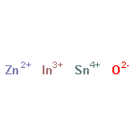
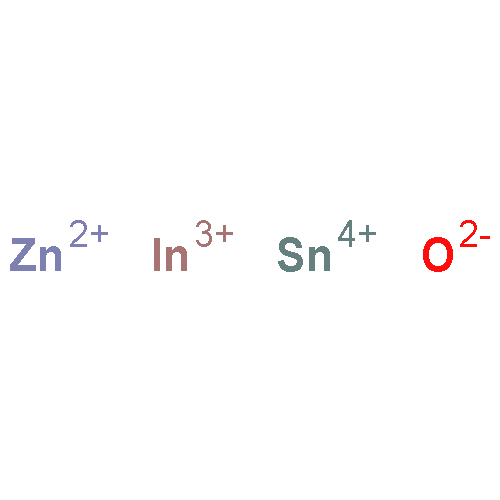
Thin films of corundum-type In2 − 2xZnxSnxO3 (cor-ZITO) were grown on lattice-matched substrates using pulsed laser deposition. The (001) of the corundum-type film grew heteroepitaxial to the (001) of a LiNbO3 substrate with large grains along the in-plane and out-of-plane orientation characterized by glancing incidence X-ray diffraction and four-circle Φ-scans. A film with 34% In (metals basis) exhibited a wide optical gap of 3.9 eV and a modest conductivity of 134 S/cm, which suggests cor-ZITO is a potential low-cost transparent conducting oxide.
Co-reporter:D.B. Buchholz, D.E. Proffit, M.D. Wisser, T.O. Mason, R.P.H. Chang
Progress in Natural Science: Materials International 2012 Volume 22(Issue 1) pp:1-6
Publication Date(Web):February 2012
DOI:10.1016/j.pnsc.2011.12.001
Zinc–indium–tin oxide (ZITO) films were grown by pulsed-laser deposition. Three different material compositions were investigated: ZITO-30, ZITO-50 and ZITO-70 in which 30%, 50% and 70%, respectively, of the indium in the In2O3 structure was replaced by substitution with zinc and tin in equal molar proportions (co-substitution): In2−2xZnxSnxO3, where x=0.3, 0.5, 0.7. All ZITO films grown at room temperature were amorphous. The first evidence of crystallinity was observed at higher deposition-temperature as the degree of co-substitution was increased. A decrease in mobility and conductivity was also observed as the degree of co-substitution was increased. The highest mobility for ZITO-30 and ZITO-50 was observed at deposition temperatures just prior to crystallization. The effect of deposition temperature on carrier concentration was minor compared to the effect of oxygen partial pressure during deposition.
Co-reporter:Michael D. Irwin, Jonathan D. Servaites, D. Bruce Buchholz, Benjamin J. Leever, Jun Liu, Jonathan D. Emery, Ming Zhang, Jung-Hwan Song, Michael F. Durstock, Arthur J. Freeman, Michael J. Bedzyk, Mark C. Hersam, Robert P. H. Chang, Mark A. Ratner, and Tobin J. Marks
Chemistry of Materials 2011 Volume 23(Issue 8) pp:2218
Publication Date(Web):April 1, 2011
DOI:10.1021/cm200229e
The functionality of NiO interfacial layers in enhancing bulk heterojunction (BHJ) organic photovoltaic (OPV) cell performance is investigated by integrated characterization of the electrical properties, microstructure, electronic structure, and optical properties of thin NiO films grown on glass/ITO electrodes. These NiO layers are found to be advantageous in BHJ OPV applications due to favorable energy band levels, interface passivation, p-type character, crystallinity, smooth surfaces, and optical transparency. The NiO overlayers are fabricated via pulsed-laser deposition and found to have a work function of ∼5.3 eV. They are investigated by both topographic and conductive atomic force microscopy and shown to passivate interfacial charge traps. The films also have an average optical transparency of >80% in the visible range, crucial for efficient OPV function, and have a near-stoichiometric Ni:O surface composition. By grazing-incidence X-ray diffraction, the NiO thin films are shown to grow preferentially in the (111) direction and to have the fcc NaCl crystal structure. Diodes of p−n structure and first-principles electronic structure calculations indicate that the NiO interlayer is preferentially conductive to holes, with a lower hole charge carrier effective mass versus that of electrons. Finally, the implications of these attributes in advancing efficiencies for state-of-the-art OPV systems—in particular, improving the open circuit voltage (VOC)—are discussed.Keywords: electron blocking layer; hole transport layer; interfacial layer; nickel oxide; NiO; organic photovoltaics; organic solar cells;
Co-reporter:Shi Qiang Li, Peijun Guo, Lingxiao Zhang, Wei Zhou, Teri W. Odom, Tamar Seideman, John B. Ketterson, and Robert P. H. Chang
ACS Nano 2011 Volume 5(Issue 11) pp:9161
Publication Date(Web):October 21, 2011
DOI:10.1021/nn203406f
This article reports the study of infrared plasmonics with both random and periodic arrays of indium–tin-oxide (ITO) nanorods (NR). A description is given on the synthesis, patterning, and characterization of physical properties of the ITO NR arrays. A classical scattering model, along with a 3-D finite-element-method and a 3-D finite-difference-time-domain numerical simulation method has been used to interpret the unique light scattering phenomena. It is also shown that the intrinsic plasma frequency can be varied through careful postsynthesis processing of the ITO NRs. Examples are given on how coupled plasmon resonances can be tuned through patterning of the ITO NR arrays. In addition, environment dielectric sensing has been demonstrated through the shift of the resonances as a result of index change surrounding the NRs. These initial results suggest potential for further improvement and opportunities to develop a good understanding of infrared plasmonics using ITO and other transparent conducting oxide semiconducting materials.Keywords: degenerate semiconductors; field enhancement; infrared plasmonics; nanorod; sensing; transparent conducting oxide
Co-reporter:Byunghong Lee, D. B. Buchholz, Peijun Guo, Dae-Kue Hwang, and R. P. H. Chang
The Journal of Physical Chemistry C 2011 Volume 115(Issue 19) pp:9787-9796
Publication Date(Web):April 27, 2011
DOI:10.1021/jp201555n
This article describes that a fluorine plasma treatment can increase the nanopore filling of a plastic electrolyte in a dye-sensitized solar cell to improve its performance. The one-step fluorine treatment can be used in a controlled way to increase the size of nanopores and nanochannels in the TiO2 nanoparticle electrode and, at the same time, passivate the TiO2 nanoparticle surfaces. In combination with the fluorine treatment, a sequential electrolyte filling process has been developed that allows the overall cell conversion efficiency to be increased by as much as 25%. The plastic-based electrolyte cells are found to be much more stable compared with their counterpart, the liquid electrolyte cells. Using this new process, and in combination with a photon confinement scheme, the overall cell efficiency can reach to about 9% using a masked frame measurement technique.
Co-reporter:Jun Liu;D. Bruce Buchholz;Antonio Facchetti;Tobin J. Marks
Advanced Materials 2010 Volume 22( Issue 21) pp:2333-2337
Publication Date(Web):
DOI:10.1002/adma.200903761
Co-reporter:Jun Liu ; D. Bruce Buchholz ; Jonathan W. Hennek ; Robert P. H. Chang ; Antonio Facchetti ;Tobin J. Marks
Journal of the American Chemical Society 2010 Volume 132(Issue 34) pp:11934-11942
Publication Date(Web):August 10, 2010
DOI:10.1021/ja9103155
Optically transparent and mechanically flexible thin-film transistors (TF-TFTs) composed exclusively of amorphous metal oxide films are fabricated on plastic substrates by combining an amorphous Ta2O5/SiOx bilayer transparent oxide insulator (TOI) gate dielectric with an amorphous zinc−indium−tin oxide (a-ZITO) transparent oxide semiconductor (TOS) channel and a-ZITO transparent oxide conductor (TOC) electrodes. The bilayer gate dielectric is fabricated by the post-cross-linking of vapor-deposited hexachlorodisiloxane-derived films to form thin SiOx layers (v-SiOx) on amorphous Ta2O5 (a-Ta2O5) films grown by ion-assisted deposition at room temperature. The a-Ta2O5/v-SiOx bilayer TOI dielectric integrates the large capacitance of the high dielectric constant a-Ta2O5 layer with the excellent dielectric/semiconductor interfacial compatibility of the v-SiOx layer in a-ZITO TOS-based TF-TFTs. These all-amorphous-oxide TF-TFTs, having a channel length and width of 100 and 2000 μm, respectively, perform far better than a-Ta2O5-only devices and exhibit saturation-regime field-effect mobilities of ∼20 cm2/V·s, on-currents >10−4 A, and current on−off ratios >105. These TFTs operate at low voltages (∼4.0 V) and exhibit good visible-region optical transparency and excellent mechanical flexibility.
Co-reporter:Jianye Li, Lung-Shen Wang, D. Bruce Buchholz and Robert P. H. Chang
Nano Letters 2009 Volume 9(Issue 5) pp:1764-1769
Publication Date(Web):March 30, 2009
DOI:10.1021/nl8035228
Through a facile and highly repeatable chemical vapor method, pure three-dimensional hyperbranched Zn3As2 structures and ultralong Ga2O3 nanowires were simultaneously grown with controllable locations in the same experiment. The hyperbranched Zn3As2 consists of cone-shaped submicro-/nanowires and has a single-crystalline tetragonal structure. This is the first report of nano Zn3As2 and hyperbranched Zn3As2 structures. The as-grown Ga2O3 nanowires are monoclinic single crystals. A vapor−solid−solid mechanism is suggested for the growth of the Ga2O3 nanowires, and a vapor-solid mechanism, for the Zn3As2 structures.
Co-reporter:D. Bruce Buchholz, Jun Liu, Tobin J. Marks, Ming Zhang and Robert P. H. Chang
ACS Applied Materials & Interfaces 2009 Volume 1(Issue 10) pp:2147
Publication Date(Web):September 18, 2009
DOI:10.1021/am900321f
Zinc−indium−tin oxide (ZITO) films are grown by pulsed-laser deposition in which 30% of the indium in the In2O3 structure is replaced by substitution with zinc and tin in equal molar proportions: In2−2xZnxSnxO3, where x = 0.3. Films grown at 25 and 100 °C exhibit electron diffraction patterns (EDPs) typical of amorphous materials. At a deposition temperature of 200 °C, evidence of crystallinity begins to appear in the EDP data and becomes more evident in films deposited at 400 °C. The advent of crystallinity affects the electrical properties of the ZITO film, and the effect is ascribed to the boundaries between phases in the films. The electrical and optical properties of the amorphous ZITO films grown at 25 °C are dependent on the oxygen partial pressure (PO2) during film growth, transitioning from a high-mobility (36 cm2/V·s) conductor (σ ∼1700 S/cm) at PO2 = 5 mTorr to a high-mobility semiconductor at PO2 ≈ 20 mTorr. Field-effect transistors (FETs) prepared with as-deposited amorphous ZITO channel layers on p+-Si/300 nm SiO2 substrates yield FETs with on/off ratios of 106, off currents of 10−8 A, and field-effect saturation mobilities of 10 cm2/V·s.Keywords: amorphous; oxide; semiconductor; transparent conducting oxide
Co-reporter:Jianye Li ; Jie Liu ; Lung-Shen Wang
Inorganic Chemistry 2008 Volume 47(Issue 22) pp:10325-10329
Publication Date(Web):October 23, 2008
DOI:10.1021/ic702427u
Wurtzitic gallium nitride nano- and microleaves were controlled grown through a facile chemical vapor deposition method. This is the first report of GaN nanoleaves, a new morphology of GaN nanostructures. The as-grown GaN structures were characterized by means of X-ray powder diffraction, scanning electron microscopy, energy dispersive X-ray, transmission electron microscopy, and selected area electron diffraction. Raman scattering spectra of the GaN leaves were studied. Field effect transistors based on individual GaN nanoleaves were fabricated, and the electrical transport results revealed a pronounced n-type gating effect of the GaN nanostructures.
Co-reporter:Robert P. H. Chang;Alexander W. Hains;Tobin J. Marks;D. Bruce Buchholz;Michael D. Irwin
PNAS 2008 Volume 105 (Issue 8 ) pp:2783-2787
Publication Date(Web):2008-02-26
DOI:10.1073/pnas.0711990105
To minimize interfacial power losses, thin (5–80 nm) layers of NiO, a p-type oxide semiconductor, are inserted between the active organic layer, poly(3-hexylthiophene) (P3HT) + [6,6]-phenyl-C61 butyric acid methyl ester (PCBM), and the ITO (tin-doped indium oxide) anode of bulk-heterojunction ITO/P3HT:PCBM/LiF/Al
solar cells. The interfacial NiO layer is deposited by pulsed laser deposition directly onto cleaned ITO, and the active layer
is subsequently deposited by spin-coating. Insertion of the NiO layer affords cell power conversion efficiencies as high as
5.2% and enhances the fill factor to 69% and the open-circuit voltage (V
oc) to 638 mV versus an ITO/P3HT:PCBM/LiF/Al control device. The value of such hole-transporting/electron-blocking interfacial
layers is clearly demonstrated and should be applicable to other organic photovoltaics.
Co-reporter:Yan Li, R.P.H. Chang
Materials Chemistry and Physics 2006 Volume 97(Issue 1) pp:23-30
Publication Date(Web):10 May 2006
DOI:10.1016/j.matchemphys.2005.06.023
Single crystal aluminum borate, including Al18B4O33 and Al4B2O9, nanowires and nanotubes have been synthesized on sapphire substrates covered by NiB powder, Pt powder and Al films. For NiB powder covered sapphire substrates, Al18B4O33 nanowires and nanotubes are formed by heating the substrates at 1100 °C under Ar gas flow. For Pt powder covered sapphire substrates, Al18B4O33 nanowires and nanotubes are produced by a chemical vapor deposition (CVD) method using boron triiodide and boric acid (BI3/H3BO3) vapor with Ar gas as precursor at 1000 °C. The nanowires are several micrometers long with diameters ranging from 50 to 200 nm, while the diameters of the nanotubes are usually larger than 200 nm. For Al film covered sapphire substrates, Al4B2O9 nanowires and nanotubes are synthesized by the CVD method using boron triiodide (BI3) vapor with Ar gas as precursor at 750–850 °C. The size of the nanostructures can be manipulated by the growth time, the growth temperature, the BI3 vapor concentration, and the Al film thickness. The nanostructure diameter and length can be varied in the range of 10–500 nm and 300 nm–2 μm, respectively. All the nanostructures have been characterized by scanning electron microscope (SEM), X-ray diffraction (XRD), transmission electron microscope (TEM), selected area electron diffraction (SAD), electron energy-loss spectrometry (EELS) and X-ray energy-dispersive spectrometry (XEDS). The growth mechanism of the aluminum borate nanowires and nanotubes is discussed.
Co-reporter:Eric W. Seelig, Betty Tang, Alexey Yamilov, Hui Cao, R.P.H. Chang
Materials Chemistry and Physics 2003 Volume 80(Issue 1) pp:257-263
Publication Date(Web):29 April 2003
DOI:10.1016/S0254-0584(02)00492-3
We present a novel method for the controlled synthesis of monodisperse ZnO colloidal spheres. These spheres are self-assembled into fcc periodic arrays. Optical measurements, including reflection-mode optical microscopy and transmission and single-domain reflection spectroscopy, reveal that the periodic arrays exhibit a photonic band gap in the (1 1 1) direction of the fcc lattice, and calculations are presented to estimate the effective value of the refractive index of the colloidal spheres. Finally, photoluminescence (PL) measurements show that the ZnO lasing thresholds are lower in periodic structures than in random arrays of identical spheres.
Co-reporter:W Fan, P.R Markworth, T.J Marks, R.P.H Chang
Materials Chemistry and Physics 2001 Volume 70(Issue 2) pp:191-196
Publication Date(Web):1 May 2001
DOI:10.1016/S0254-0584(00)00502-2
Homoepitaxial magnesium oxide thin films have been grown on MgO(1 0 0), (1 1 0) and (1 1 1) substrates by the plasma enhanced metal-organic chemical vapor deposition. Atomic force microscopy measurements indicate that the as-received MgO substrate surface morphology is greatly improved as a result of MgO homoepitaxial growth. Various oxygen partial pressures and plasma powers were selected to investigate the role of atomic oxygen species during the growth of the MgO thin films. Oxygen plasma conditions were analyzed by Langmuir probe measurements. These studies reveal that higher concentrations of atomic oxygen effectively assist the layer-by-layer growth kinetics, which are critical to generating atomically flat surfaces. Smooth surfaces, with roughness as low as 0.036 nm, are achieved on MgO(1 0 0) substrates under the conditions of 2.1 mTorr oxygen partial pressure and 1300 W plasma power at 720°C.
Co-reporter:Stephen Loser, Sylvia J. Lou, Brett M. Savoie, Carson J. Bruns, Amod Timalsina, Matthew J. Leonardi, Jeremy Smith, Tobias Harschneck, Riccardo Turrisi, Nanjia Zhou, Charlotte L. Stern, Amy A. Sarjeant, Antonio Facchetti, Robert P. H. Chang, Samuel I. Stupp, Mark A. Ratner, Lin X. Chen and Tobin J. Marks
Journal of Materials Chemistry A 2017 - vol. 5(Issue 19) pp:NaN9232-9232
Publication Date(Web):2017/04/19
DOI:10.1039/C7TA02037F
Improved understanding of fundamental structure–property relationships, particularly the effects of molecular shape and intermolecular packing on film morphology and active layer charge transport characteristics, enables more rational synthesis of new p-type small molecules. Here we investigate a series of small molecules consisting of an acene-based electron-rich core flanked by one or two electron-deficient diketopyrrolopyrrole (DPP) moieties. Through minor changes in the molecule structures, measurable variations in the crystal structure and sizable differences in macroscopic properties are achieved. The molecular symmetry as well as the conformation of the side chains affects the unit cell packing density and strength of the intermolecular electronic coupling in single crystals of all molecules in this series. The addition of a second DPP unit to the benzodithiophene (BDT) core increases molecular planarity leading to decreased reorganization energy, strong cofacial coupling, and moderate hole mobility (2.7 × 10⁻⁴ cm2 V−1 s−1). Increasing the length of the acene core from benzodithiophene to naphthodithiophene (NDT) results in a further reduction in reorganization energy and formation of smaller crystalline domains (∼11 nm) when mixed with PCBM. Decreasing the aspect ratio of the core using a “zig-zag” naphthodithiophene (zNDT) isomer results in the highest hole mobility of 1.3 × 10⁻³ cm2 V−1 s−1 due in part to tight lamellar (d = 13.5 Å) and π–π stacking (d = 3.9 Å). The hole mobility is directly correlated with the short-circuit current (11.7 mA cm−2) and solar cell efficiency (4.4%) of the highest performing zNDT:PCBM device. For each of these small molecules the calculated π-coupling constant is correlated with the hole mobility as a function of crystal structure and orientation indicating the importance of designing molecules that create extended crystalline networks with maximal π-orbital overlap.
Co-reporter:Xinge Yu, Nanjia Zhou, Shijiao Han, Hui Lin, Donald B. Buchholz, Junsheng Yu, Robert P. H. Chang, Tobin J. Marks and Antonio Facchetti
Journal of Materials Chemistry A 2013 - vol. 1(Issue 40) pp:NaN6535-6535
Publication Date(Web):2013/08/29
DOI:10.1039/C3TC31412J
Flexible ammonia (NH3) gas sensors based on solution-processable organic thin-film transistors (OTFTs) are fabricated using a TIPS-pentacene active layer/PMMA dielectric layer on glass and plastic substrates. These OTFT sensors exhibit outstanding NH3 gas response and recovery characteristics under multiple exposure/evacuation cycles at controlled NH3 concentrations.
.jpg)
![Benzo[1,?2-?b:4,?5-?b']?dithiophene, 2,?6-?dibromo-?4,?8-?bis[5-?(2-?ethylhexyl)?-?2-?thienyl]?-](http://img.cochemist.com/ccimg/1482500/1482447-24-4.png)
![Benzo[1,?2-?b:4,?5-?b']?dithiophene, 2,?6-?dibromo-?4,?8-?bis[5-?(2-?ethylhexyl)?-?2-?thienyl]?-](http://img.cochemist.com/ccimg/1482500/1482447-24-4_b.png)
![Stannane, 1,1'-[4,8-bis[5-(2-ethylhexyl)-2-thienyl]benzo[1,2-b:4,5-b']dithiophene-2,6-diyl]bis[1,1,1-trimethyl-](/data/chemimg/139400/1352642-37-5.png)
![Stannane, 1,1'-[4,8-bis[5-(2-ethylhexyl)-2-thienyl]benzo[1,2-b:4,5-b']dithiophene-2,6-diyl]bis[1,1,1-trimethyl-](/data/chemimg/139400/1352642-37-5_b.png)
![Zincate(1-), [4-[2-[15-[bis(4-hexylphenyl)amino]-10,20-bis[2,6-bis(octyloxy)phenyl]-21H,23H-porphin-5-yl-κN21,κN22,κN23,κN24]ethynyl]benzoato(3-)]-,](/data/chemimg/101000/1350928-18-5.png)
![Zincate(1-), [4-[2-[15-[bis(4-hexylphenyl)amino]-10,20-bis[2,6-bis(octyloxy)phenyl]-21H,23H-porphin-5-yl-κN21,κN22,κN23,κN24]ethynyl]benzoato(3-)]-,](/data/chemimg/101000/1350928-18-5_b.png)
![Pyrrolo[3,4-c]pyrrole-1,4-dione, 3,6-bis(5-bromo-2-thienyl)-2,5-dihydro-2,5-bis(2-octyldodecyl)-](/data/chemimg/139000/1260685-63-9.png)
![Pyrrolo[3,4-c]pyrrole-1,4-dione, 3,6-bis(5-bromo-2-thienyl)-2,5-dihydro-2,5-bis(2-octyldodecyl)-](/data/chemimg/139000/1260685-63-9_b.png)
![Pyrrolo[3,4-c]pyrrole-1,4-dione, 3,6-bis(5-bromo-2-thienyl)-2,5-bis(2-butyloctyl)-2,5-dihydro-](/data/chemimg/2260700/1224709-68-5.png)
![Pyrrolo[3,4-c]pyrrole-1,4-dione, 3,6-bis(5-bromo-2-thienyl)-2,5-bis(2-butyloctyl)-2,5-dihydro-](/data/chemimg/2260700/1224709-68-5_b.png)


![Benzo[1,2-b:4,5-b']dithiophene, 4,8-bis[5-(2-ethylhexyl)-2-thienyl]-](/data/chemimg/139500/1352642-35-3.png)
![Benzo[1,2-b:4,5-b']dithiophene, 4,8-bis[5-(2-ethylhexyl)-2-thienyl]-](/data/chemimg/139500/1352642-35-3_b.png)
![2-Ethylhexyl 4,6-dibromo-3-fluorothieno[3,4-b]thiophene-2-carboxylate](http://img.cochemist.com/ccimg/1237500/1237479-39-8.png)
![2-Ethylhexyl 4,6-dibromo-3-fluorothieno[3,4-b]thiophene-2-carboxylate](http://img.cochemist.com/ccimg/1237500/1237479-39-8_b.png)
![Benzo[1,2-b:4,5-b']dithiophene, 2,6-dibromo-4,8-bis[(2-ethylhexyl)oxy]-](/data/chemimg/380400/1226782-13-3.png)
![Benzo[1,2-b:4,5-b']dithiophene, 2,6-dibromo-4,8-bis[(2-ethylhexyl)oxy]-](/data/chemimg/380400/1226782-13-3_b.png)
![Anthra[2,1,9-def:6,5,10-d'e'f']diisoquinoline-5-carbonitrile, 12-bromo-2,9-bis(2-ethylhexyl)-1,2,3,8,9,10-hexahydro-1,3,8,10-tetraoxo-](/data/chemimg/139400/1198360-51-8.png)
![Anthra[2,1,9-def:6,5,10-d'e'f']diisoquinoline-5-carbonitrile, 12-bromo-2,9-bis(2-ethylhexyl)-1,2,3,8,9,10-hexahydro-1,3,8,10-tetraoxo-](/data/chemimg/139400/1198360-51-8_b.png)


![Anthra[2,1,9-def:6,5,10-d'e'f']diisoquinoline-1,3,8,10(2H,9H)-tetrone, 5,12-dibromo-2,9-bis(2-ethylhexyl)-](/data/chemimg/102800/851786-15-7.png)
![Anthra[2,1,9-def:6,5,10-d'e'f']diisoquinoline-1,3,8,10(2H,9H)-tetrone, 5,12-dibromo-2,9-bis(2-ethylhexyl)-](/data/chemimg/102800/851786-15-7_b.png)
![4H-Thieno[3,4-c]pyrrole-4,6(5H)-dione, 5-octyl-](/data/chemimg/112100/773881-43-9.png)
![4H-Thieno[3,4-c]pyrrole-4,6(5H)-dione, 5-octyl-](/data/chemimg/112100/773881-43-9_b.png)
![2,5-Bis(trimethylstannyl)thieno[3,2-b]thiophene](http://img.cochemist.com/ccimg/470000/469912-82-1.png)
![2,5-Bis(trimethylstannyl)thieno[3,2-b]thiophene](http://img.cochemist.com/ccimg/470000/469912-82-1_b.png)


![3-Heptanone, 5-[(2-methoxyethyl)imino]-2,2,6,6-tetramethyl-](http://img.cochemist.com/ccimg/151300/151225-57-9.png)
![3-Heptanone, 5-[(2-methoxyethyl)imino]-2,2,6,6-tetramethyl-](http://img.cochemist.com/ccimg/151300/151225-57-9_b.png)

![Stannane, [2,2'-bithiophen]-5-yltrimethyl-](http://img.cochemist.com/ccimg/133200/133144-35-1.png)
![Stannane, [2,2'-bithiophen]-5-yltrimethyl-](http://img.cochemist.com/ccimg/133200/133144-35-1_b.png)
![1,2-Ethanediamine, N'-ethyl-N,N-bis[2-(ethylamino)ethyl]-](http://img.cochemist.com/ccimg/124800/124764-04-1.png)
![1,2-Ethanediamine, N'-ethyl-N,N-bis[2-(ethylamino)ethyl]-](http://img.cochemist.com/ccimg/124800/124764-04-1_b.png)
![Perbromothieno[3,2-b]thiophene](http://img.cochemist.com/ccimg/124700/124638-53-5.png)
![Perbromothieno[3,2-b]thiophene](http://img.cochemist.com/ccimg/124700/124638-53-5_b.png)
![Erbium Tris[bis(trimethylsilyl)amide]](http://img.cochemist.com/ccimg/103500/103457-72-3.png)
![Erbium Tris[bis(trimethylsilyl)amide]](http://img.cochemist.com/ccimg/103500/103457-72-3_b.png)
![Anthra[2,1,9-def:6,5,10-d'e'f']diisoquinoline-1,3,8,10(2H,9H)-tetrone, 2,9-dioctyl-](/data/chemimg/709500/78151-58-3.png)
![Anthra[2,1,9-def:6,5,10-d'e'f']diisoquinoline-1,3,8,10(2H,9H)-tetrone, 2,9-dioctyl-](/data/chemimg/709500/78151-58-3_b.png)


![2,5-Bis(2-ethylhexyl)-3,6-di(thiophen-2-yl)pyrrolo[3,4-c]pyrrole-1,4(2H,5H)-dione](http://img.cochemist.com/ccimg/1185900/1185885-86-2.png)
![2,5-Bis(2-ethylhexyl)-3,6-di(thiophen-2-yl)pyrrolo[3,4-c]pyrrole-1,4(2H,5H)-dione](http://img.cochemist.com/ccimg/1185900/1185885-86-2_b.png)
![dithieno[3,2-c:2',3'-e]oxepine-4,6-dione](http://img.cochemist.com/ccimg/1043100/1043023-52-4.png)
![dithieno[3,2-c:2',3'-e]oxepine-4,6-dione](http://img.cochemist.com/ccimg/1043100/1043023-52-4_b.png)


![Pyrrolo[3,4-c]pyrrole-1,4-dione, 3-(5-bromo-2-thienyl)-2,5-bis(2-ethylhexyl)-2,5-dihydro-6-(2-thienyl)-](/data/chemimg/139400/1308671-90-0.png)
![Pyrrolo[3,4-c]pyrrole-1,4-dione, 3-(5-bromo-2-thienyl)-2,5-bis(2-ethylhexyl)-2,5-dihydro-6-(2-thienyl)-](/data/chemimg/139400/1308671-90-0_b.png)