BASIC PARAMETERS Find an error
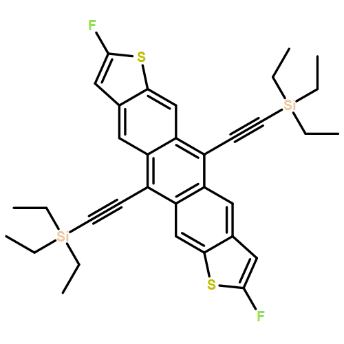
Anthradithiophene chromophores are found in many current high-performance organic semiconductors, even though these materials are typically synthesized as an inseparable mixture of syn and anti isomers. Recent syntheses of pure syn anthradithiophenes have shown no improvement in performance for the more homogeneous system, but similar studies on the pure anti isomer have not been reported. In this work, a simple protocol is described to prepare the pure anti isomer of fluorinated, functionalized anthradithiophenes, and perform detailed analysis of the intermolecular interactions in the crystal that yield increased density and closer chromophore contacts. Studies of the charge-transport properties of these pure isomers, compared to the isomeric mixtures, suggest that the benefit of isomer purity is not consistent; in the syn case, there was minimal difference between the pure isomer and the mixture, while for the anti isomer mobility improved nearly twofold. Analysis of disorder in the crystals suggests a reason for this difference in performance.
The preparation of uniform large-area highly crystalline organic semiconductor thin films that show outstanding carrier mobilities remains a challenge in the field of organic electronics, including organic field-effect transistors. Quantitative control over the drying speed during dip-coating permits optimization of the organic semiconductor film formation, although the kinetics of crystallization at the air–solution–substrate contact line are still not well understood. Here, we report the facile one-step growth of self-aligning, highly crystalline soluble acene crystal arrays that exhibit excellent field-effect mobilities (up to 1.5 cm V−1 s−1) via an optimized dip-coating process. We discover that optimized acene crystals grew at a particular substrate lifting-rate in the presence of low boiling point solvents, such as dichloromethane (b.p. of 40.0 °C) or chloroform (b.p. of 60.4 °C). Variable-temperature dip-coating experiments using various solvents and lift rates are performed to elucidate the crystallization behavior. This bottom-up study of soluble acene crystal growth during dip-coating provides conditions under which one may obtain uniform organic semiconductor crystal arrays with high crystallinity and mobilities over large substrate areas, regardless of the substrate geometry (wafer substrates or cylinder-shaped substrates).
Fluorination has been demonstrated to improve stability and processing in thiophene-containing small-molecule semiconductors. Here, the impact of partial fluorination on these parameters in a pentacene derivative is examined. Although the improvement in photostability is not as dramatic, there is a clear improvement in the stability of the chromophore upon fluorination. The improvement in processability is more dramatic; devices formed by spin-coating with the fluorinated derivative perform substantially better than those formed from the nonfluorinated compound.
Understanding the interactions at interfaces between the materials constituting consecutive layers within organic thin-film transistors (OTFTs) is vital for optimizing charge injection and transport, tuning thin-film microstructure, and designing new materials. Here, the influence of the interactions at the interface between a halogenated organic semiconductor (OSC) thin film and a halogenated self-assembled monolayer on the formation of the crystalline texture directly affecting the performance of OTFTs is explored. By correlating the results from microbeam grazing incidence wide angle X-ray scattering (μGIWAXS) measurements of structure and texture with OTFT characteristics, two or more interaction paths between the terminating atoms of the semiconductor and the halogenated surface are found to be vital to templating a highly ordered morphology in the first layer. These interactions are effective when the separating distance is lower than 2.5 dw, where dw represents the van der Waals distance. The ability to modulate charge carrier transport by several orders of magnitude by promoting “edge-on” versus “face-on” molecular orientation and crystallographic textures in OSCs is demonstrated. It is found that the “edge-on” self-assembly of molecules forms uniform, (001) lamellar-textured crystallites which promote high charge carrier mobility, and that charge transport suffers as the fraction of the “face-on” oriented crystallites increases.
Scalable manufacturing of small-molecule organic thin film transistors (OTFTs) with performance approaching single crystals requires extraordinary control over microstructures and morphologies of organic semiconductors (OSCs). Here, contact-induced nucleation in the context of small-molecule OSCs and OSC:polymer blends prepared by blade coating, a printing process capable of mimicking large area batch and roll-to-roll manufacturing, is investigated. Using polarized optical microscopy, microbeam grazing incidence wide angle X-ray scattering, and energy-filtered transmission electron microscopy, it is revealed that previous design rules drawn from spin coating of OSCs and contact-induced nucleation may have to be revisited in the context of blade coating. It is shown that blade coating achieves texture purity in case of 2,8-difluoro-5,11-bis(triethylsilylethynyl) anthradithiophene (diF-TES-ADT), irrespective of whether the contact is chemically treated with a halogenated self-assembled monolayer (SAM) or not, in contrast to spin coating which requires an SAM. Here, it is demonstrated that OSC–contact interactions increase the nucleation density and can disrupt the vertical stratification in polymer:OSC blends with great detrimental effects on carrier transport. Using these lessons, we demonstrate bottom-contact bottom-gate OTFTs without chemical surface modification achieving hole mobilities of 4.6 and 3.6 cm2 V−1 s−1, using 6,13-bis(triisopropylsilylethynyl)pentacene and diF-TES-ADT, respectively, blended with an insulating polymer.
Blending of small-molecule organic semiconductors (OSCs) with amorphous polymers is known to yield high performance organic thin film transistors (OTFTs). Vertical stratification of the OSC and polymer binder into well-defined layers is crucial in such systems and their vertical order determines whether the coating is compatible with a top and/or a bottom gate OTFT configuration. Here, we investigate the formation of blends prepared via spin-coating in conditions which yield bilayer and trilayer stratifications. We use a combination of in situ experimental and computational tools to study the competing effects of formulation thermodynamics and process kinetics in mediating the final vertical stratification. It is shown that trilayer stratification (OSC/polymer/OSC) is the thermodynamically favored configuration and that formation of the buried OSC layer can be kinetically inhibited in certain conditions of spin-coating, resulting in a bilayer stack instead. The analysis reveals here that preferential loss of the OSC, combined with early aggregation of the polymer phase due to rapid drying, inhibit the formation of the buried OSC layer. The fluid dynamics and drying kinetics are then moderated during spin-coating to promote trilayer stratification with a high quality buried OSC layer which yields unusually high mobility >2 cm2 V−1 s−1 in the bottom-gate top-contact configuration.
Solution-processable functionalized acenes have received special attention as promising organic semiconductors in recent years because of their superior intermolecular interactions and solution-processability, and provide useful benchmarks for organic field-effect transistors (OFETs). Charge-carrier transport in organic semiconductor thin films is governed by their morphologies and molecular orientation, so self-assembly of these functionalized acenes during solution processing is an important challenge. This article discusses the charge-carrier transport characteristics of solution-processed functionalized acene transistors and, in particular, focuses on the fine control of the films' morphologies and structural evolution during film-deposition processes such as inkjet printing and post-deposition annealing. We discuss strategies for controlling morphologies and crystalline microstructure of soluble acenes with a view to fabricating high-performance OFETs.
The phase-separation characteristics of spin-cast difluorinated-triethylsilylethynyl anthradithiophene (F-TESADT)/poly(methyl methacrylate) (PMMA) blends are investigated with the aim of fabricating transistors with a high field-effect mobility and stability. It is found that the presence of PMMA in the F-TESADT/PMMA blends prevents dewetting of F-TESADT from the substrate and provides a platform for F-TESADT molecules to segregate and crystallize at the air–film interface. By controlling the solvent evaporation rate of the spin-cast blend solution, it is possible to regulate the phase separation of the two components, which in turn determines the structural development of the F-TESADT crystals on PMMA. At a low solvent evaporation rate, a bilayer structure consisting of highly ordered F-TESAT crystals on the top and low-trap PMMA dielectric on the bottom can be fabricated by a one-step spin-casting process. The use of F-TESADT/PMMA blend films in bottom gate transistors produces much higher field-effect mobilities and greater stability than homo F-TESADT films because the phase-separated interface provides an efficient pathway for charge transport.